Systems-on-a-Chip Research Projects
Current Projects
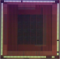
Next Generation Computing (Sept. 2012-Sept. 2014)Lincoln Laboratory - Huy Nguyen MIT Lincoln Laboratory has been funding a collaborative research effort with Prof. Arvind Mithal to investigate next-generation computing accelerators and architectures for high-performance computing. The first years of the collaboration involved the development of a million-point Sparse FFT kernel first demonstrated by campus in FPGAs and is currently being implemented in ASIC form by MIT Lincoln Laboratory. MIT is currently investigating high-bandwidth memory architectures for flash memory using custom FPGA controllers. Such architectures could be useful for non-volatile integrated memory on chips or for big data computing platforms. |
|
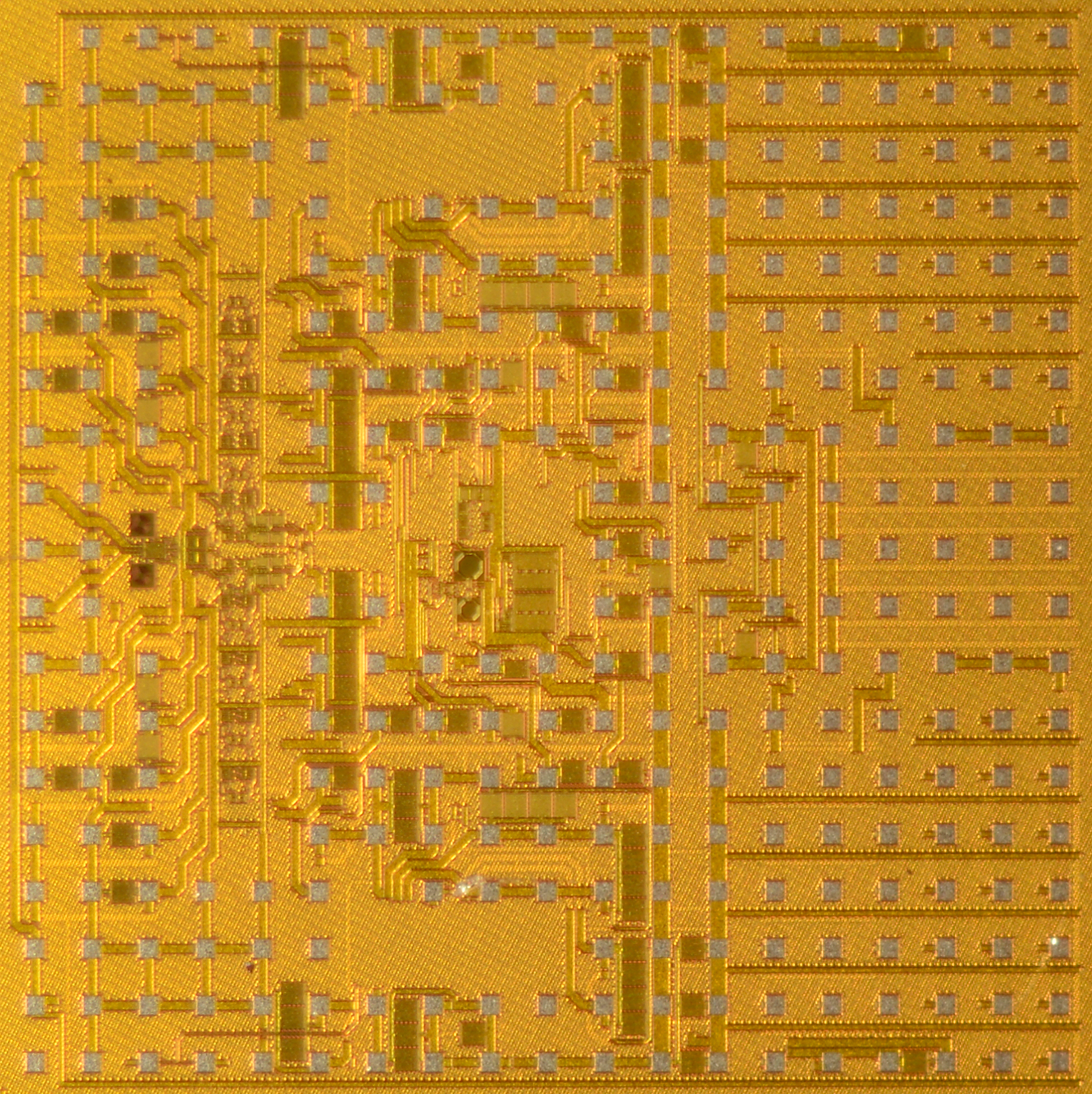
RF/Mixed-Signal SoCs (Sept. 2013 - Present)Lincoln Laboratory - Timothy Hancock & Xiao Wang MIT and MIT Lincoln Laboratory have been collaborating on two mixed-signal IC design projects. The first involves the development of a transcranial Doppler system for diagnostic use in patients with neurotrauma, cerebrovascular accident (i.e., stroke), and other neurovascular pathologies to monitor patient state. The system employs multi-channel transceiver electronics and a two-dimensional transducer array to enable steering of the ultrasound beam. Electronic beam steering allows for algorithmic vessel location, thereby obviating the need for manual transducer alignment and operator expertise. The second project is related to the non-linear equalization of analog/mixed systems. The equalization is achieved by estimating a set of nonlinear coefficients through the proper choice of excitation waveforms. By removing the system nonlinearities through the use of equalization, the overall system can be made more linear, thus improving overall performance or the reduction of the power consumption of the system. |
|
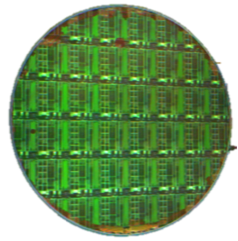
Integrated Photonics (Sept. 2011 - Sept. 2014)Lincoln Laboratory - Paul Juodawlkis Researchers in the MIT Research Laboratory of Electronics (RLE) and the Advanced Technology Division at Lincoln Laboratory have been collaborating on the DARPA Electronic-Photonic Heterogeneous Integration (E-PHI) program to develop a 3D integration platform containing CMOS electronic, silicon photonics, and compound-semiconductor laser sources. For the E-PHI program, the CMOS electronics wafers were fabricated in Lincoln Laboratory's Microelectronics Laboratory and the silicon photonics wafers were fabricated using an external foundry. The electronics and photonics wafers are being integrated using the Laboratory's wafer-scale 3D integration process. A high-power, single-frequency laser source is also being integrated onto the platform by combining a novel slab-coupled optical waveguide amplifier (SCOWA) and a distributed Bragg reflector (DBR) grating fabricated in a silicon-nitride waveguide. Lincoln Laboratory also has the capability to fabricate silicon and compound-semiconductor photonic integrated circuits (PICs) using internal cleanroom facilities. |
 |


